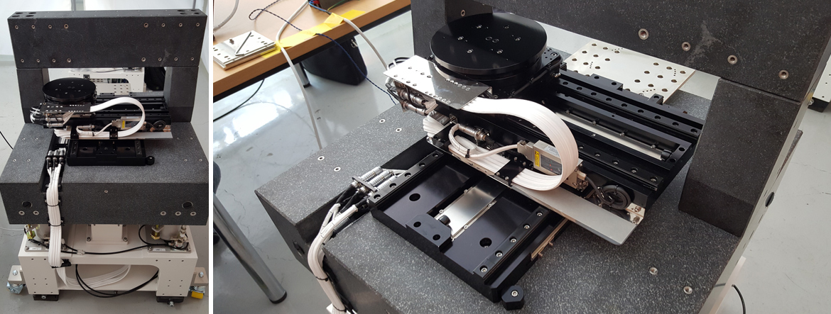
Semiconductor
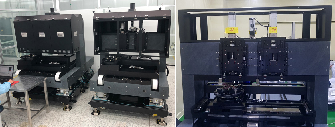
Nano Inspection
The stage is used for the inspection equipment of inner and outer defects of Si wafer or glass substrate.
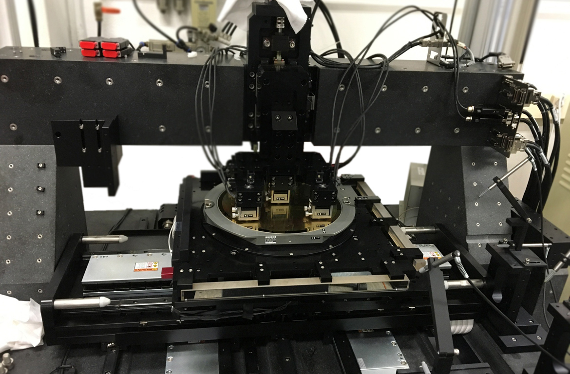
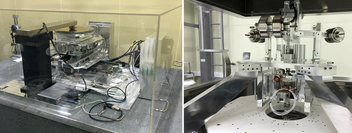
Overlay
This is the stage used in the technical equipment to detect the transverse deformation error of the pattern by using the stacked layers of the Si wafer.
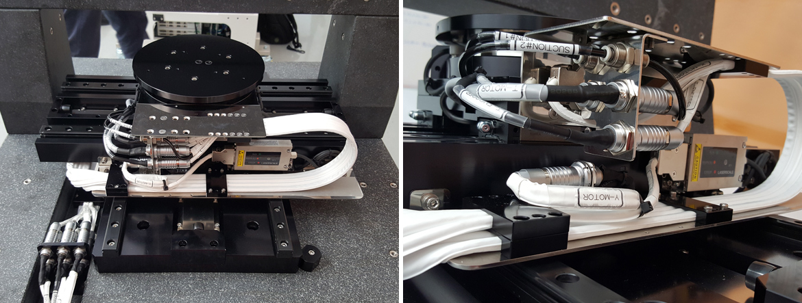
Vacuum Stage
Ultra-precision vacuum stage that can be used for inspection equipment equipped with vacuum system in semiconductor process
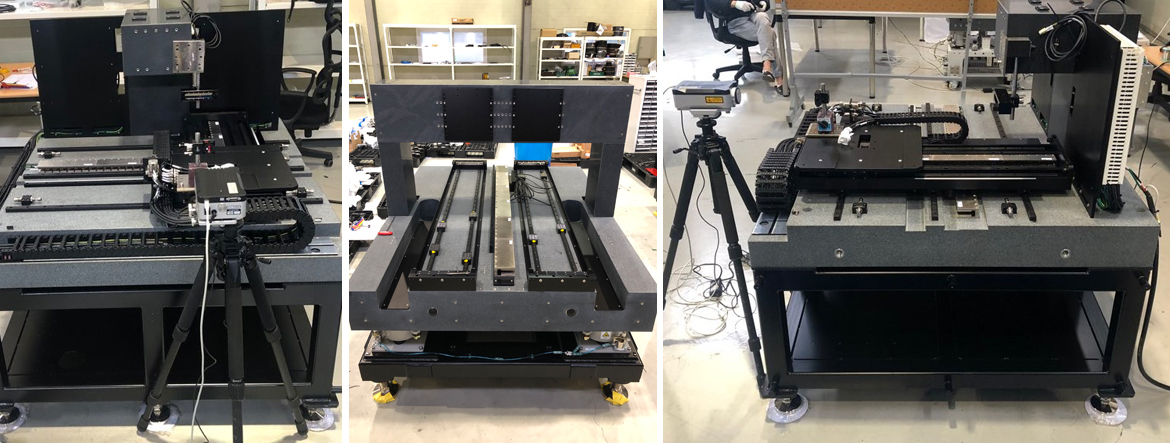
Other inspection
This stage is used for the inspection equipment in micrometer(um) units where the defect size on the Si wafer is larger than nanometer(nm).